- 您现在的位置:买卖IC网 > Sheet目录1993 > DS1394U-33+T&R (Maxim Integrated Products)IC RTC SPI 3WIRE W/CHRGR 10-MSOP
DS1390–DS1394
Low-Voltage SPI/3-Wire RTCs with
Trickle Charger
20
Maxim Integrated
SPI Serial-Data Bus
The DS1390/DS1391/DS1394 provide a 4-wire SPI seri-
al-data bus to communicate in systems with an SPI host
controller. The DS1390/DS1391 support SPI modes 1
and 3, while the DS1394 supports SPI modes 0 and 2.
Both devices support single-byte and multiple-byte
data transfers for maximum flexibility. The DIN and
DOUT pins are the serial-data input and output pins,
respectively. The CS input initiates and terminates a
data transfer. The SCLK pin synchronizes data move-
ment between the master (microcontroller) and the
slave (DS1390/DS1391) devices. The shift clock
(SCLK), which is generated by the microcontroller, is
active only during address and data transfer to any
device on the SPI bus. Input data (DIN) is latched on
the internal strobe edge and output data (DOUT) is
shifted out on the shift edge (Figure 9). There is one
clock for each bit transferred. Address and data bits
are transferred in groups of eight.
Address and data bytes are shifted MSB first into the
serial-data input (DIN) and out of the serial-data output
(DOUT). Any transfer requires the address of the byte
to specify a write or read, followed by one or more
bytes of data. Data is transferred out of the DOUT pin
for a read operation and into the DIN for a write opera-
tion (Figures 10 and 11).
The address byte is always the first byte entered after
CS is driven low. The most significant bit (W/R) of this
byte determines if a read or write takes place. If W/R is
0, one or more read cycles occur. If W/R is 1, one or
more write cycles occur.
Data transfers can occur one byte at a time or in multi-
ple-byte burst mode. After CS is driven low, an address
is written to the DS1390/DS1391/DS1394. After the
address, one or more data bytes can be written or
read. For a single-byte transfer, one byte is read or writ-
ten and then CS is driven high. For a multiple-byte
transfer, however, multiple bytes can be read or written
after the address has been written. Each read or write
cycle causes the RTC register address to automatically
increment. Incrementing continues until the device is
disabled. The address wraps to 00h after incrementing
to 0Fh (during a read) and wraps to 80h after incre-
menting to 8Fh (during a write). Note, however, that an
updated copy of the time is only loaded into the user-
accessible copy upon the falling edge of CS. Reading
the RTC registers in a continuous loop does not show
the time advancing.
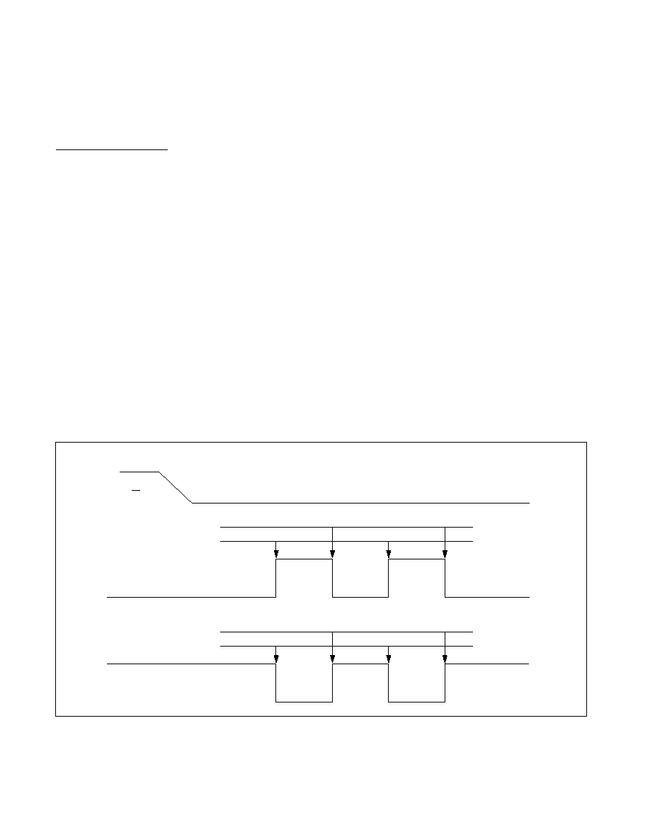
CPHA = 0
CPHA = 1
CS
SHIFT DATA OUT (READ)
MODE 0
MODE 2
DATA LATCH/SAMPLE (WRITE)
SCLK WHEN CPOL = 0
SHIFT DATA OUT (READ)
DATA LATCH/SAMPLE (WRITE)
MODE 1
MODE 3
SHIFT DATA OUT (READ)
DATA LATCH/SAMPLE (WRITE)
SHIFT DATA OUT (READ)
SCLK WHEN CPOL = 1
Figure 9. Serial Clock as a Function of Microcontroller Clock-Polarity Bit
发布紧急采购,3分钟左右您将得到回复。
相关PDF资料
DS14285SN+T&R
IC RTC W/NV RAM CNTRL 24-SOIC
DS1486P-120+
IC TIMEKEEPER RAM 1MB 34-PCM
DS1500WE
IC RTC Y2KC W/NV CTRL 32-TSOP
DS1501YSN+T&R
IC RTC WDOG Y2K 5V IND 28-SOIC
DS1553P-70+
IC RTC RAM Y2K 5V 70NS 34-PCM
DS1554W-120IND
IC RTC RAM Y2K 3.3V 120NS 32EDIP
DS1556WP-120IND
IC RTC RAM Y2K 3.3V 120NS 34PCM
DS1557P-70IND
IC RTC RAM Y2K 5V 70NS 34PCM
相关代理商/技术参数
DS1395
制造商:DALLAS 制造商全称:Dallas Semiconductor 功能描述:RAMified Real Time Clock
DS1395N
制造商:未知厂家 制造商全称:未知厂家 功能描述:Peripheral IC
DS1395S
制造商:DALLAS 制造商全称:Dallas Semiconductor 功能描述:RAMified Real Time Clock
DS1395SN
制造商:未知厂家 制造商全称:未知厂家 功能描述:Peripheral IC
DS1397
制造商:DALLAS 制造商全称:Dallas Semiconductor 功能描述:RAMified Real Time Clock
DS-14
功能描述:非热缩管和套管 FLEX BRAIDED SHIELD 14MM X 100M ROLL
RoHS:否 制造商:Panduit 产品:Cable Wraps 类型:Spiral 颜色:Black 材料:PP 内径:0.03 in 长度:100 ft
DS14-00
制造商:FLOWLINE 功能描述:Sensor, Liquid Level, Ultrasonic Switch/Control 4 Relays; Range 49.2 in, 1NPT
DS1-40-0001
制造商:SCHURTER 制造商全称:Schurter Inc. 功能描述:Storage Choke, fully potted resign